







Professor Sofer of UCT Prague contributed to an international Nature study on programmable materials
The work was carried out as part of an international collaboration between leading research institutions, including the Massachusetts Institute of Technology (MIT) and the U.S. Department of Energy’s Oak Ridge National Laboratory. The combination of state-of-the-art experimental techniques, theoretical modeling, and materials chemistry made it possible to achieve a result that had previously been considered technologically out of reach.
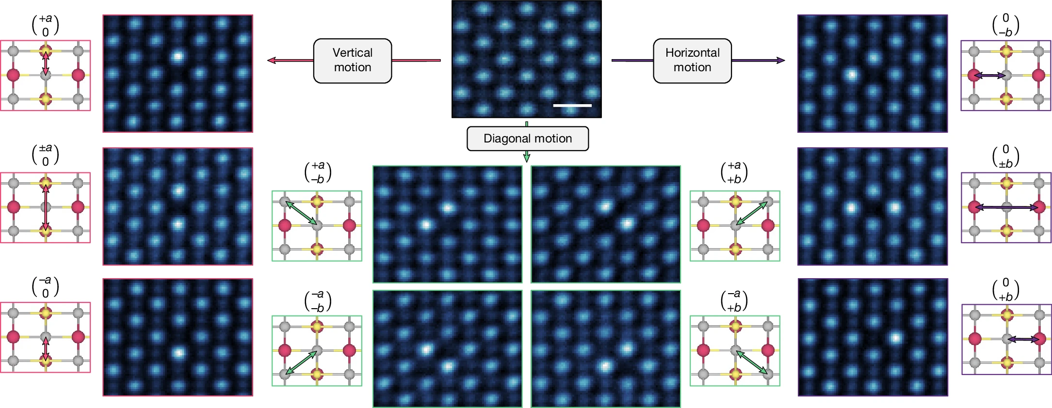
While earlier techniques primarily allowed atomic manipulation on material surfaces, this new study demonstrates, for the first time, deterministic control of atoms inside a three-dimensional crystal lattice. Using highly precise electron beam, the researchers were able to reposition individual atoms at specific lattice sites and create more than 40,000 controlled defects within a single crystal in a matter of minutes.
These engineered “defects” are not imperfections but rather a key to new material functionalities, ranging from optical to quantum properties. The result is a new class of so-called artificial matter that can be, to a certain extent, “programmed.”
Professor Zdeněk Sofer of UCT Prague is among the co-authors of the study. His research group has long focused on the synthesis and investigation of advanced materials, particularly semiconductors and two-dimensional (2D) materials.
“Our research group is primarily focused on the synthesis of single crystals and nanostructures of 2D materials. In this work, we provided high-quality CrSBr single crystals with an exceptionally low defect density, enabling the creation of precisely defined atomic-scale defects. This material combines unique optical and magnetic properties, and our laboratory is among the few worldwide capable of producing it in the required quantity and purity,” says Professor Sofer.
The ability to deliberately “program” materials at the atomic level opens up a wide range of potential applications in optoelectronics and quantum technologies. The approach is relatively universal and can also be applied to materials with different structures, such as AgCrP2S6, where magnetic one-dimensional structures can be formed. Importantly, the engineered structures are stable at room temperature, representing a key step toward practical applications. Moreover, single-crystalline CrSBr combines unique magnetic, electronic, structural, and optical properties with sufficient chemical stability.
The results of the study indicate that the future of materials engineering lies not only in selecting materials but increasingly in their deliberate design at the atomic scale.
The research was carried out within the INTER-EXCELLENCE II project funded by the Ministry of Education, Youth and Sports (LUAUS25268) and the publication can be accessed here:
https://www.nature.com/articles/s41586-026-10431-9